
DSPBrik™ II X6A1250 Wideband ADC with FPGA (BECOMING DEPRECATED)
Description
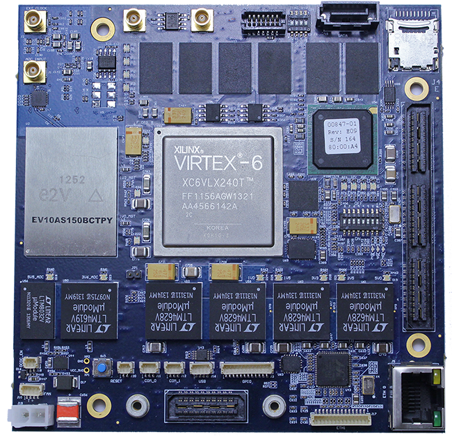
The DSPBrik™ II X6A1250 analog-to-digital converter (ADC) card is becoming deprecated. It combines a 10 bit analog-to-digital converter, with a large FPGA for high-performance digital signal processing. The ADC samples at up to 2.6 GSPS and has a 10 MHz to 5 GHz input passband, enabling digitization of signals in multiple Nyquist zones. The FPGA and ADC are controlled via an on-board microprocessor running embedded Linux.
The X6A1250 is ideal for acquiring wideband satellite communication signals. A typical application includes direct digitization of an L-band (950 MHz to 1750 MHz) output from a microwave block down converter.
Once the signal is digitized, the FPGA can be used to implement a number of different functions, such as sub-band tuning, demodulation, channelization, and spectral analysis. Processed data can be sent to other systems via multiple 10GbE interfaces. The X6A1250 is used as a core component of the DLSR2.
Features
- Wide analog input bandwidth (10 MHz to 5 GHz)
- Digitize L band directly from a down converter (800 MHz bandwidth)
- Xilinx Virtex-6 FPGA for data processing and precision time tagging
- 2 GByte DDR3 SDRAM attached to the Virtex-6 FPGA
- Programmable on-board 600 MHz to 2.6 GHz clock generator, with internal or external 10 MHz reference
- Precision time tagging of sampled data via NMEA-0183 or IRIG-B time code and 1 PPS inputs
- 800 MHz, NXP P1010 Processor with 1 GByte SDRAM and Rincon Research Corporation’s embedded Linux distribution
- 10/100/1000 Ethernet interface for command and control operation
- One high-speed DSPBrik™II connector utilizing LVDS signaling
- One high-speed SERDES connector attached to eight Virtex-6 GTX transceivers capable of various serial formats (RXAUI/XAUI/SGMII/PCIe)
- 4.6 inch square form factor
- Connectivity with DSPBrik II family products
Documentation
For more information, download the DSPBrik II Family Product Brief.
Order
Orderable Part Numbers:
- X6A1250-L240C2 Wideband ADC with Virtex-6 XC6VLX240T-2C FPGA
- X6A1250-S315C2 Wideband ADC with Virtex-6 XC6VSX315T-2C FPGA
- X6A1250-S475C2 Wideband ADC with Virtex-6 XC6VSX475T-2C FPGA
Other configurations are possible. Please contact us if you are interested in customizing a product to your specific requirements.
Orders may be placed via e-mail, telephone, fax, or mail.
Commercial Price List available upon request.
E-mail: sales@rincon.com
Phone: 520-519-3131
Fax: 520-519-3120
Mail: Rincon Research Corporation
Attention: Sales
101 North Wilmot Road, Suite 101
Tucson, AZ 85711
WARNING: Commodities, including associated software, firmware, and technical data, offered for sale on this site are controlled for export by the U.S. Department of State under the International Traffic in Arms Regulations (ITAR) or by the Department of Commerce under the Export Administration Regulations (EAR). Purchaser is required by U.S. law to comply with these regulations. Export, re-export, and retransfer of these commodities by any means without the required licenses or other U.S. Government authorization is prohibited by U.S. law.
Technical Specifications
ADC
e2v EV10AS150B
Analog Input Level
+15 dBm full-scale at 16 dB default attenuation, AC coupled
Analog Input Bandwidth
10 MHz to 5 GHz
Input Impedance/Connector
50 Ω MCX
ENOB
7.8 bit
Programmable Attenuation
1 dB to 32 dB, 0.5 dB steps
FPGA SDRAM
2 GByte (4 devices, 512 MBytes each)
Microprocessor SDRAM
1 GByte (2 devices, 512 MBytes each)
microSD/SDHC card user/field replaceable
Parallel Connector
One Samtec QSH-060-01-L-D-DP-A
Speed: 1000MHz / bit
Signal Level: LVDS
Width: 44 data bit, 4 Clocks
Serial Connector
One Samtec QSH-020-01-L-D-DP-A
Signal Level: CML
Signal Capabilities: RXAUI, XAUI, PCIe, SGMII
Accuracy
+/- 1 ADC sampling clock cycle
NMEA-0183
RS-232 input, 9600 baud, 3 wire, 2 mm connector
IRIG-B
0.5 Vpp to 10 Vpp input range (AGC controlled), 50/604 Ω, MCX
1 PPS
LVCMOS level, 50/10 kΩ input termination, rise/fall edge (selectable), MCX
External Reference/Clock
Ref: 10 MHz sinusoidal/square wave, 750 mVpp to 2 Vpp
Clock: 1200 MHz to 2500 MHz, +8 dBm to +20 dBm, sine wave, DC coupled
50 Ω, MCX
Dimensions & Weight
4.6” L x 4.6” W x 1½” H, 4.75 oz
Operating Voltage
9 VDC to 16 VDC, 12 VDC (nom)
Power Connector
Molex 2-pin Mini-Fit Jr.
Operating Temperature
0°C to +50°C